For the chips in our computers and smartphones to get faster and faster, their components - the circuits and wires through which signals flow - have to get smaller and smaller.
The miniaturization of these wires has taken scientists on a journey almost to the atomic level. Recently, scientists have begun to address - and now to surmount - certain barriers in physics that have prevented them from making even smaller wires.
In a recent study, a team of researchers from the U.S. Department of Energy's Argonne National Laboratory (DOE), the University of Chicago, and MIT has developed a new way to create some of the world's thinnest wires, using a process that could enable mass manufacturing with standard types of equipment.
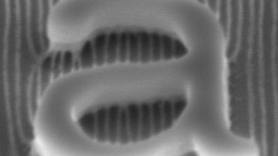
Templated assembly, or directed self-assembly, as it is known, represents an easier and more cost-effective way to make nanowires with widths below 10 nanometers (about 100 atoms thick).
The self-assembling materials are large molecules known as block copolymers. These block copolymers are the two-headed beasts of the chemical world - one end is water-loving, the other end is water-hating.
Upon heating, they spontaneously form highly uniform structures at the molecular scale.
On their own, however, the block copolymers would form a pattern that looks like a fingerprint or a piece of brain coral - useless for the creation of functional nanowires.
The key to changing that pattern to something more ordered is the use of the chemically patterned templates.
Past approaches to making tiny ordered nanostructures used expensive specialized optics to direct extreme wavelengths of light or electron beams to write patterns line-by-line.
The new approach involves creating a chemical pattern as a template using these same tools at relatively low resolution, and then filling in the template to fabricate high-resolution patterns using a self-assembling material.
For very high-resolution block copolymer systems, a "topcoat" is often added during the process. This topcoat constrains the way the block copolymers self-assemble, forcing them into a regular, ordered structure perpendicular to the surface they are grown on.
"Think of it like baking a cake," said Argonne nanoscientist Leonidas Ocola, a co-author of the study. "Without a mold for the cake, it can bake in a shape you don't want it to bake. Having the mold gives it that shape that you want. The mold creates boundary conditions needed to define the shape you want."
"The topcoat and underlying lithographic pattern work together to guide the formation of the nanostructure and provide the morphology we want," he added.
Although self-assembling materials in nanomanufacturing have been known for quite a while, using block copolymers with the topcoat enables patterns for dense arrays of tiny wires.
"A systems-level understanding of the template, topcoat and self-assembling block copolymer is the key to the whole process - you need to find a way to induce the block copolymer film to assembly into desired architectures for manufacturing, and be able to transfer the pattern of the block copolymer into the actual device materials, such as semiconducting silicon wires or conducting copper wires," said Paul Nealey, Brady W. Dougan Professor in Molecular Engineering at the Institute for Molecular Engineering at the University of Chicago and another author of the study.
Because the topcoat polymer layer does not need to be removed prior to pattern transfer steps, and additional layers can be patterned on top of the topcoat, the system can be used to build up many kinds of complex patterns, as would be needed for the interconnections of a microchip.
Most microchip manufacturing facilities use existing lithographic methods, and the chemical vapor deposition process used to create the topcoat is itself a well-understood additional step that could be added relatively easily. Thus, implementing the new method could be much more straightforward than other proposed methods of making finer lines.
With the new method, "you wouldn't need to change all those machines," said co-author Karen Gleason, MIT associate provost and Alexander and I. Michael Kasser Professor of Chemical Engineering. "And everything that's involved are well-known materials."
