Microencapsulation, in which a tiny particle of one material is encased within a shell made from another, is widely used in pharmaceuticals manufacturing and holds promise for other areas, such as self-repairing materials and solar power.
But most applications of microencapsulation require particles of uniform size, and that's something that existing fabrication techniques don't reliably provide. In products with a high profit margin, such as pharmaceuticals, it can be cost effective to mechanically separate particles of the proper size from those that are too large or too small, but in niche or small-margin products, it may not be.
In the latest issue of the journal Lab on a Chip, researchers from MIT's Microsystems Technology Laboratories report a new microencapsulation technique that yields particles of very consistent size, while also affording a high rate of production.
Moreover, the devices used to produce the spheres were themselves manufactured with an affordable commercial 3-D printer. The ability to 3-D print fabrication systems would not only keep manufacturing costs low but also allow researchers to quickly develop systems for producing microencapsulated particles for particular applications.
"When you print your microsystems, you can iterate them very fast," says Luis Fernando Velásquez-García, a principal research scientist in the Microsystems Technology Laboratories and senior author on the new paper. "In one year, we were able to make three different generations that are significantly different from one another and that in terms of performance also improve significantly. Something like that would be too expensive and too time consuming with other methods."
Velásquez-García is joined on the paper by Daniel Olvera-Trejo, a postdoc at Mexico's Tecnológico de Monterrey who was a visiting researcher at MIT under the auspices of a new nanoscience research partnership between the two universities.
Concentric Circles
The researchers' new system adapts the same core technology that Velásquez-García's group has previously explored as a means for depositing material on chip surfaces, etching chips, generating X-rays, spinning out nanofibers for use in a huge range of applications, and even propelling nanosatellites.
All of these applications rely on dense arrays of emitters that eject fluids, electrons, or streams of ions. The emitters might be conical, cylindrical, or rectangular; etched microscopically or 3-D printed; hollow, like nozzles, or solid. But in all instances, Velásquez-García's group has used electric fields -- rather than, say, microfluidic pumps -- to control their emissions.
The new emitters are a variant on the hollow 3-D-printed design. But instead of having a single opening at its tip, each emitter has two openings -- a hole and a concentric ring. The openings are fed by separate microfluidic channels. If the viscosity and electrical conductivity of the fluids fed through the channels, the strength of the electric field that draws them up, and the length and diameter of the channels are precisely calibrated, the emitters will produce tiny spheres in which the material drawn through the outer ring encases the material drawn through the center hole.
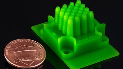
According to Velásquez-García, the physics describing the relationship of forces that produces the microcapsules is only around a decade old. Other researchers have built individual emitters that can produce microcapsules, but Velásquez-García's group is the first to arrange the emitters in a monolithic array -- 25 emitters packed onto a chip that's less than an inch square -- while maintaining both efficiency and uniformity. The arrays are also modular in design, so they can be tiled together to produce larger arrays.
Pharmaceuticals manufacturers use microencapsulation to protect drugs from degradation before they reach their targets. But researchers have also explored microencapsulation as a way to make self-healing materials: The same stress that causes a material to crack would break the capsules, releasing an epoxy that would patch the crack. There, uniformity of capsule size is crucial to ensure that distributing the capsules throughout the material doesn't compromise its structural integrity.
Dye-sensitized solar cells, another potential application for the new technique, are potentially a cheap alternative to silicon solar cells. They use tiny particles of dye-coated metal suspended in some other material, often a fluid. The dye converts light to electricity, which the metal transmits to electrodes. Preserving an exact ratio of dye-covered surface area to volume of metal maximizes the efficiency of the cell.
Printing Possibilities
In their initial experiments, Velásquez-García and Olvera-Trejo used water and sesame oil as their fluids, and the emitters were made from plastic. The resulting microspheres were around 25 micrometers in diameter. There are, however, 3-D printers that use metal or ceramics, which could produce emitters able to tolerate hotter or harsher fluids.
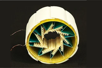
To pack the emitter arrays into the smallest possible volume, the researchers used helical fluid channels, which spiral around the interiors of the emitters, minimizing their height. To control the rate of emission, the channels also taper, from 0.7 millimeters at their bases to 0.4 mm at their tips. Such small and complex devices would be virtually impossible to manufacture using standard microfabrication processes, Velásquez-García says.
"These devices can only be made if you print them," Velásquez-García says. "We're not doing printing because we can. We're doing printing because it enables something that didn't exist before that brings very exciting possibilities."